
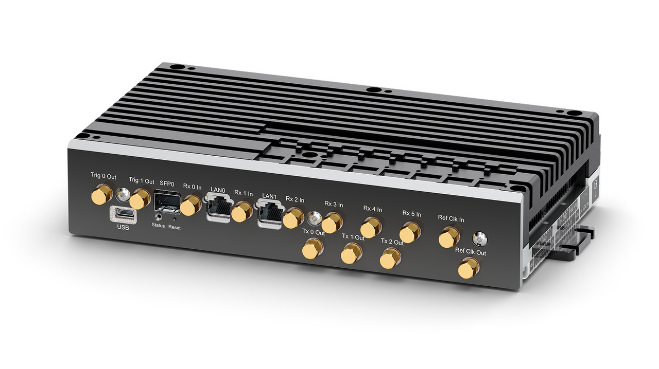
IFDR10 specifications
| Function | Description |
|---|---|
| IF bandpass filter |
Programmable digital FIR with software‑selectable bandwidth. Built-in filter design software with user interface. |
| Characteristic | Description |
|---|---|
| A/D and D/A conversion |
Resolution: 16 bit Sampling rate: 190 … 240 MHz (software-selectable) |
| Dynamic range (dependent on matched filter) |
104 dB without compression (1 µs pulse) 107 dB without compression (2 µs pulse) |
| IF range | 10 ... 120 MHz |
| Input signals |
|
| Master clock jitter |
< 0.5 picosec, integrated over 200 Hz ... 2 MHz offset |
| Multiply/accumulate cycles per second | 448 billion |
| Pulse repetition frequency (PRF) | 50 Hz ... 20 kHz, +0.1 %, continuously selectable |
|
Saturation level (1 dB compression) |
+13.3 dBm at 50 Ω |
| Characteristic | Description |
|---|---|
Three Tx outputs |
10 ... 120 MHz +13dBm @ 60Ω |
| Characteristic | Description |
|---|---|
| Inputs | Only digital inputs |
| AFC output |
Serial control output Automatic 2D (time/frequency) burst pulse search and fine-tracking algorithms |
| Data output through Ethernet | 32-bit floating point I and Q values |
| I/O interface |
8 independent GPIO pairs Each pair can be configured as one differential input/output, or as two single-ended inputs/outputs (max 16 single-ended lines) |
| IFDR10 to RVP10SRV link | Optical link (10 Gbit) |
| Charasteristic | Description |
|---|---|
| Minimum high level input voltage | 3.5 V |
| Maximum low level input voltage | 1.5 V |
| Absolute maximum input voltage | 5.0 V |
| Absolute minimum input voltage | 0.0 V |
| Charasteristic | Description |
|---|---|
| Output voltage high | 5.0 V (I out = 0 mA) |
| 4.3 V (I out = -10 mA) | |
| 3.6 V (I out = -20 mA) | |
| Output voltage low | 0.0 V (I out = 0 mA) |
| 0.7 V (I out = 10 mA) | |
| 1.4 V (I out = 20 mA) |
| Characteristic | Decription |
|---|---|
| Differential input threshold voltage | -200 … +200 mV |
| Absolute maximum and minimum differential input voltage | ±5 V |
| Absolute maximum input voltage to gnd | 5.0 V |
| Absolute minimum input voltage to gnd | 0.0 V |
| Common mode voltage to gnd if not limited by absolute max/min input voltage | 0.0 … 5.0 V |
| Typical differential output voltage high | 4.1 V (I out = 0 mA) |
| 2.8 V (I out = 10 mA) | |
| 2.3 V (I out = 20 mA) | |
| Typical differential output voltage low | -4.1 V (I out = 0 mA) |
| -2.8 V (I out = 10 mA) | |
| -2.3 V (I out = 20 mA) |
The differential GPIO voltage of a pin pair is defined as the Odd pin voltage minus the Even pin voltage. For example, if GPIO1 = 2 V and GPIO0 = 0.3 V, the differential GPIO voltage is 2 V – 0.3 V = 1.7 V, and the differential pin state is true.