Adjusting burst spectra and AFC plot when using passband filter or matched filter
- Make sure you have successfully captured the burst pulse with the Pb command.
- Type the Ps command.
-
Use the space bar to display the burst spectrum plot by itself, and use the
Z key to shift the entire graph into view.
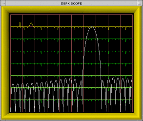
The plot shows the frequency content of the transmitted pulse.
- Check that the plot shows a clean main power lobe centered at the receivers intermediate frequency.
- Check the spectrum for spurious harmonics, excessive width, and other out-of-band noise.
- Adjustment the transmitter to give a sharper main lobe or reduce spurious noise.
-
Begin designing the passband FIR filter.
Use the space bar to display both the filter response and the burst spectrum on the same plot.
Use the Z key to shift the bursts main lobe up to the top horizontal line of the graph. This makes it level with the filters peak lobe, which is always drawn tangent to the same top line.
Figure 1. Example of a poorly designed passband filter 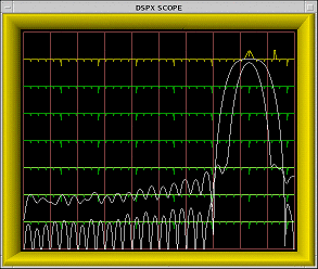
Begin with the FIR length that was chosen previously in the Pb command. When using the passband filter, begin with the N and W keys to set an initial bandwidth equal to the reciprocal of the pulse width.
-
The main lobes of the two plots should more-or-less overlap. Experiment with changing
the FIR length and bandwidth to achieve a filter with the following properties.
- The filter width should be no greater than the burst spectral width. A wider passband reduces the SNR of the received signal because out-of-band noise would be allowed to pass.
- The DC gain should be as small as possible, preferably less than -65 dB.
- If there are conspicuous interference spikes at particular frequencies, try to adjust the location of the filter’s zeros so that the interference is maximally attenuated.
-
Optimize the performance of the FIR filter.
When using the matched filter, much of this work is automated for you. Make sure that the pulselength value in themw menu section is set correctly, so that the entirety of the pulse is captured in the pb plot. The matching bandwidth given the pulse length will be calculated and applied to the matched filter for you. You may also use the F key to iterate through the windowing functions to find the one that provides the best matching shape to your burst pulse.
The filter should not pass any frequencies that do not contain useful information from the original transmitted pulse. If anything, choose a filter whose width is slightly narrower than the bursts spectral width.
The previous figure shows an example of a filter that is poorly matched to the pulse. Although the filter has fairly good DC rejection, it passes frequencies that are outside of the transmitter's broadcast range. These frequencies only bring noise to the synthesized I and Q data stream.
You can optimize the passband FIR filter manually:
Defining a nearly optimal filter requires a few minutes of hunting with the I, W, and N keys. Each time you press any of these keys, RVP10 designs a new FIR filter from scratch, and displays the results. Even though you must still control two degrees of freedom (length and bandwidth), the RVP10 design calculations perform several hundred iterative steps each time, which preferentially select for the best filter. Because the FIR coefficients are quantized in the filter chips themselves, the process of finding an optimal filter becomes quite nonlinear.
Example
The offset error of the IFDR A/D converter is at most 10mV, that is, -27 dBm into its 50 Ω input.
To achieve 90 dB of dynamic range below the converters +8 dBm saturation level, we expect usable I and Q values to be obtainable from a (sub-LSB) input signal at -82 dBm. This is 55 dB below the interference that would result from the worst-case A/D offset.
But a weak input signal at -82 dBm would still be damaged by even an equal level of DC interference. Therefore, adding another 10 dB safety margin, we get -65 dB as the recommended maximum DC gain of the matched filter. This DC gain should be reduced even further if it is known that coherent leakage is present in the receive signal at a level greater than the -27 dBm worse-case A/D offset.
The following figure shows a 60 MHz filter with particularly poor (-42 dB) DC rejection. The frequency range of the plot is 36 MHz to 72 MHz, therefore, DC appears aliased at the right edge and we can see a peak in the filters stopband at DC. Contrast this with the filter shown previously that has a true zero at DC. In general, a poor filter can be significantly improved by making only incremental changes to the impulse response length and/or desired bandwidth.